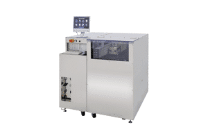
Large samples mechanical profilometer FP Series 1. Large samples from 200 to 500mm 2. KLA measuring heads 3. Sub-nanometric vertical precision 4. Long sweep strokes 5. Repositioning of high reproducibility Toho Technology offers surface metrology solutions suitable for large samples (from 200 to 500mm). Using KLA measurement heads, FP series performance achieves sub-nanometric vertical accuracy. […]
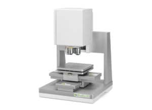
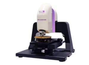
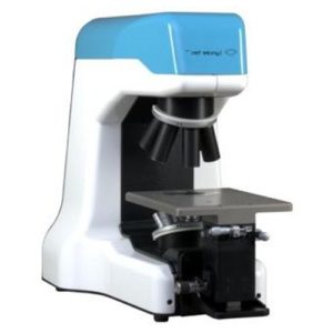
Optical profilometer at the best quality / price Profilm3D 1. Sub-nanometric vertical resolution with 500µm piezoelectric scanning 2. Vertical scanning interferometry (VSI) and phase shift (PSI) 3. Advanced analysis software 4. Motorized stage 5. Objective detection 6. Easy to use 7. Stiching function Finally, measurements of surface roughness and topography can be made with an […]
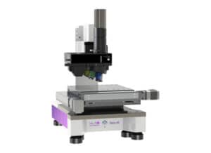
Optical profilometer for R&D Zeta-20 1. Versatility and Performance 2. Punctual measurement 3. High resolution 3D topography in color even on transparent sample 4. Interferometric: white light VSI – Nomarski – PSI 5. Thickness of transparent thin layers The Zeta-20 is a fully integrated optical profilometer that provides 3D metrology and imaging capacity in a […]
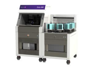
Automated optical profilometer, large sample Zeta-388 1. For industry 2. Automated measurement 3. High resolution 3D topography in color even on transparent sample 4. Interferometric: white light VSI – Nomarski – PSI 5. Thickness of transparent thin layers The Zeta-388 offers metrology and 3D imaging capability, combined with an integrated isolation table and a cassette-to-cassette […]
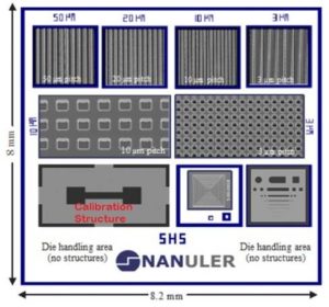
Standards Calibration – Standard step Nanuler Calibration Standard This versatile calibration standard is designed for the calibration of AFM, SEM, optical and mechanical profilers. Features include step heights, lines, grids, magnification box, and measurement structures of different tones. The characteristics are engraved in SiO2 and Si and are optionally available with a metallic coating for […]
Optical profilometer for industry MicroXAM 800 1. For industry 2. Automated measurement on several sites 3. VSI & PSI white light 4. Interferometric: white light VSI – Nomarski – PSI 5. Simple and flexible The MicroXAM-800 is an optical profiler based on a white light interferometer which measures nanometer level characteristics with phase scanning interferometry […]
Profilometer for stress measurement FLX 2320 S 1. For industry 2. Mass production 3.Thin film stress measurement 4. Temperature from -65 ° C to 500 ° C 5. Fast Toho FLX-2320-S Thin Film Stress Measurement Systems offer industry standard capabilities for serial and research installations that require precise strain measurements on various films and substrates […]
DHM microscope – Materials science DHM R Serie 1. Non-contact scanning 2. 3D profilometry at an unrivaled speed 3. MEMS analysis, up to 25 MHz 4. Measure under controlled environmental conditions 5. Measure the topography of transparent patterns The DHM Reflection series (DHM®-R1000, DHM®-R2100 and DHM®-R2200) are holographic microscopes configured in reflection. They are ideal […]
DHM microscope – Life science DHM T Serie 1. Non-invasive 2. Study unexplored biological processes 3. Perform multimodal imaging 4. Optical profilometer configured for transmission 5. Study innovative materials and devices Transmission DHM® measures the difference in optical path of a beam passing through samples. For measurements of micro-optical components, microfluidic devices and defects or […]
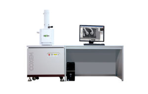
Table Top scanning electron microscopes EM-30 Serie 1. Intuitive user interface 2. Automatic functions – Motorized sample support along 3 axes (X, Y, T) – Auto focus, contrast, brightness, alignment of the electron gun 3. Maximum sample size up to 70mm in diameter and 45mm in height 4. Magnification from x20 to x150,000 (Resolution from […]
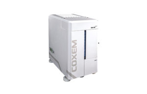
Standard scanning electron microscopes CX-200 Series 1. Intuitive user interface 2. Full automatic functions (X, Y, R, T, Z axes) or partly manual 3. The large room can accommodate up to 160mm (W) * 55mm (H) 4. Magnification of x 300,000 (20nm resolution at 30kV) 5. Quick replacement of a sample in less than two […]
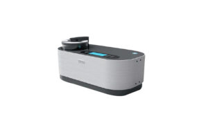
SEM sample metallizer SPT-20 1. Easy to use 2. Digital interface 3. Adaptation to each samples Non-conductive samples often have a charge effect due to the accumulation of electrons on the surface, which poses problems for collecting a good image. Although SEM’s “low vacuum” or “load reduction” mode can overcome this problem, this mode generally […]


